CHINESE
 ENGLISH
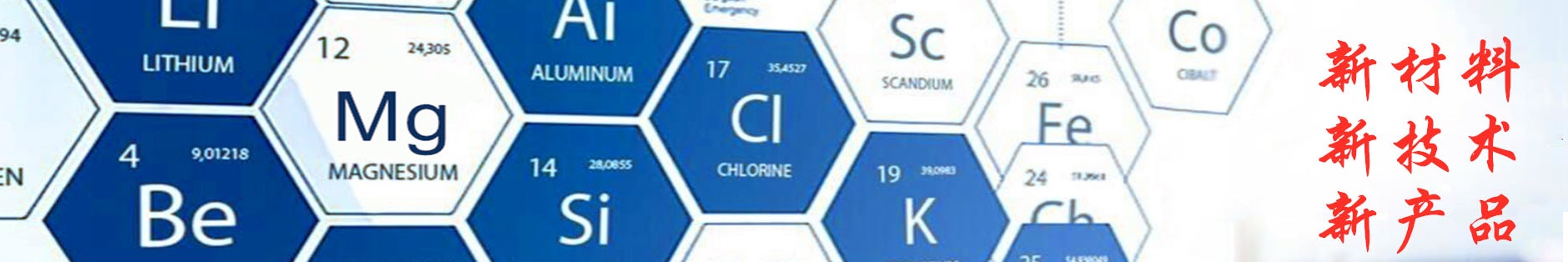
Products >> Rare metal & Wafers >> Gallium series

Gallium Phosphide GaP
- Product No.:pmp42
Gallium Phosphide GaP wafer
Special order is workable! We can also supply other diameter Gap wafer according to customer's requirement.Plz mail to [email protected] for details!
Contact:Jason Wang Mobile:+86-18039202132 (whatsapp.wechat)
Email:[email protected]
GaP wafer /GaP Powder/GaP Granule
Product introduction
CHINA ALLOY NEW STEVERS CO,LTD.supply GaP monocrystal materials with volume production, unique monocrystal growth control method, and the complete GaP monocrystal production line. Its products are mainly used in LED of ordinary light such as red, yellow, and green, which is as one of the primary substrates of LED.
CHINA ALLOY NEW STEVERS CO,LTD.supply GaP monocrystal materials with volume production, unique monocrystal growth control method, and the complete GaP monocrystal production line. Its products are mainly used in LED of ordinary light such as red, yellow, and green, which is as one of the primary substrates of LED.
Specifications and parameters
|
Product
|
GaP monocrystal
|
||
|
Dopant
|
S
|
Te
|
None
|
|
Carrier concentration cm-3
|
(2~7)×1017
|
(1~2)×1017
|
|
|
Mobility cm2/v.s
|
≥100
|
||
|
EPD cm-2
|
<2×10⁵
|
||
|
Diameter mm
|
50±0.5, 50.8±0.5
|
||
|
Thickness µm
|
300 ± 20
|
||
|
Crystal orientation
|
(111)±0.5°
|
||
|
Wafer surface state
|
Slice, grinding, corrosion, polishing
|
||
Special order is workable! We can also supply other diameter Gap wafer according to customer's requirement.Plz mail to [email protected] for details!
Contact:Jason Wang Mobile:+86-18039202132 (whatsapp.wechat)
Email:[email protected]
Next Product:GaN wafer
Products Category
Contact Us

Name: Jason Wang
Tel: +86-18039202132
E-mail: [email protected]
Add: Material Industrial Park, Science avenue, Zhengzhou, Henan, China

 Mail inquiry